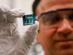
NEW YORK - A team led by an Indian-origin engineer from the University of Utah has discovered a new kind of 2D semi-conducting material for electronics that opens the door for much speedier computers and smartphones that consume a lot less power. The semi-conductor, made of the elements tin and oxygen or tin monoxide (SnO) by the associate professor Ashutosh Tiwari-led team is a layer of 2D material only one atom thick,

allowing electrical charges to move through it much faster than conventional 3D materials such as silicon. This material could be used in transistors, the lifeblood of all electronic devices such as computer processors and graphics processors in desktop computers and mobile devices. Transistors and other components used in electronic devices are currently made of 3D materials such as silicon and consist of multiple layers on a glass substrate. But the downside to 3D materials is that electrons bounce around inside the layers in all directions.
“The benefit of 2D materials is that the material is made of one layer the thickness of just one or two atoms. Consequently, the electrons can only move in one layer so it's much faster,” Tiwari said. Transistors made with Tiwari's semi-conducting material could lead to computers and smartphones that are over 100 times faster than regular devices. “Because the electrons move through one layer instead of bouncing around in a 3D material, there will be less friction, meaning the processors will not get as hot as normal computer chips,” the authors noted. They will also require much less power to run, a boon for mobile electronics that have to run on battery power.
According to Tiwari, this could be especially important for medical devices such as electronic implants that will run longer on a single battery charge. Now that Tiwari and his team have discovered this new 2D material, it can lead to the manufacturing of transistors that are even smaller and faster than those in use today. A computer processor is comprised of billions of transistors, and the more transistors packed into a single chip, the more powerful the processor can become.
“The field is very hot right now and people are very interested in it," Tiwari said, adding that in two or three years, we should see at least some prototype device. The paper describing the material was published in the journal Advanced Electronic Materials.

 RSS Feed
